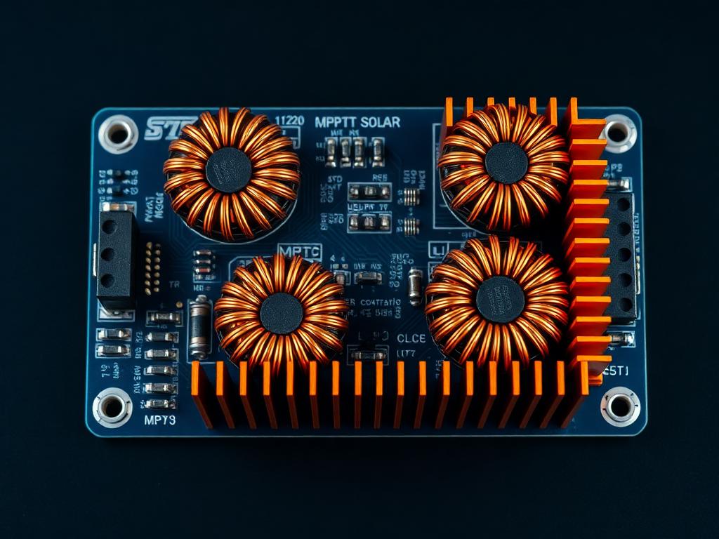
PCB design
Multi-layer board design
Schematic capture, layout and DFM review tuned for performance, cost and manufacturability from day one.


Grouped the way the work actually flows: design, build, prove. A product moves from schematic to shipped unit inside a single operation.
Not a list of separate services. Each stage feeds the next, which is what removes lead time, handoff risk and cost from the programme.
Multi-layer board and custom silicon design, with firmware engineered alongside the hardware it runs on.
Bring us a specification →PCB design
Schematic capture, layout and DFM review tuned for performance, cost and manufacturability from day one.
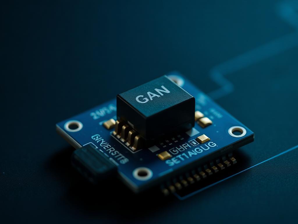
Silicon
Custom device work and applied research targeting power conversion efficiency in African operating conditions.
End-to-end production from component sourcing to final assembly, at volumes that let OEMs scale.
Tour the facility →
Assembly
Surface-mount and through-hole lines with automated placement, reflow and inspection.
Packaging
Device packaging, enclosure integration and full box-build ready for distribution.
Every unit verified before it leaves the line, and supported into the systems it powers.
Talk to engineering →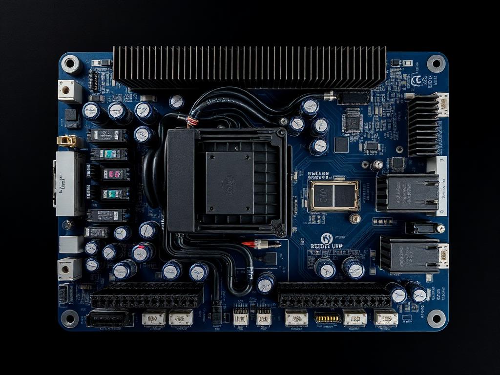
Quality
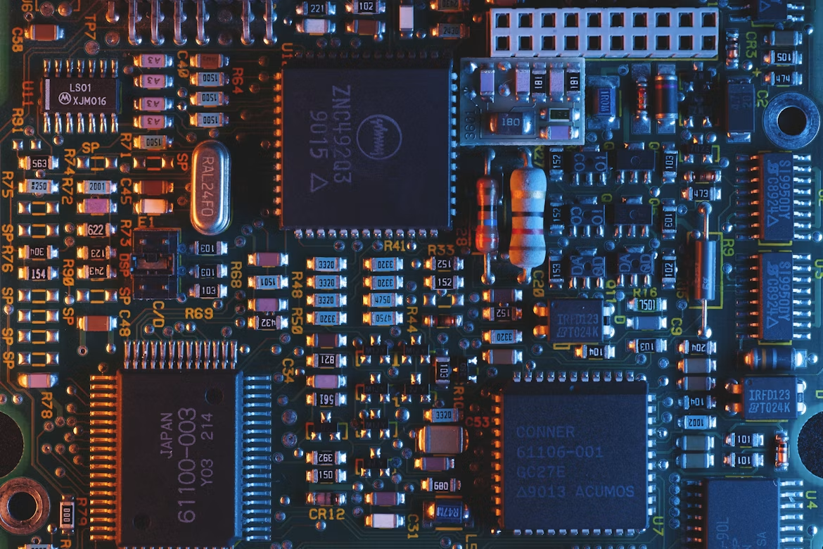
Functional test, burn-in and compliance verification against the standards each market demands.
Support
Traceability, documentation and delivery support from the line into deployed systems.
When design, build and test sit under one roof, a design change does not restart a procurement cycle on another continent. Iterations happen in days, not quarters.
Tell us what you're building and where it has to ship.